The Atomic Semi Technical Assessment: Portable Silicon Fabrication in 2026
Atomic Semi is a venture-backed startup co-founded by Sam Zeloof and industry veteran Jim Keller that aims to decentralise semiconductor manufacturing. By building small, portable "mini-fabs," the com

The Pitch
Atomic Semi is a venture-backed startup co-founded by Sam Zeloof and industry veteran Jim Keller that aims to decentralise semiconductor manufacturing. By building small, portable "mini-fabs," the company intends to enable rapid iteration from "atoms to architecture" for custom silicon. It positions itself as an artisanal alternative to the multi-billion dollar mega-fabs that currently dominate the industry.
Under the Hood
The core technical premise relies on using recycled semiconductor equipment and photolithography to create functioning integrated circuits outside of a traditional cleanroom (Source: YouTube). While Zeloof’s early work focused on Z1 and Z2 chips with roughly 1,200 transistors, the company is now scaling operations and actively hiring Process Development Engineers in San Francisco (Source: BuiltIn, April 2026). Funding has been secured through Fontinalis Partners and other institutional investors (Source: Tracxn).
However, the "backyard" approach faces several critical technical hurdles that limit its utility for modern backend infrastructure:
- Scaling: The process is currently limited to micron-scale features, making it unsuitable for the sub-5nm logic required by models like GPT-5 or Claude 4.5 (Source: SemiAnalysis).
- Yield: Operating without a professional-grade cleanroom leads to high defect rates, specifically drain-to-source shorts caused by particle contamination (Source: TechSpot).
- Safety: The fabrication process requires handling hazardous chemicals, including Hydrofluoric Acid, in non-industrial settings (Source: YouTube).
- Density: We don't know the maximum bit-density for their "home-made" RAM cells as the data remains proprietary (Source: UsedBy Dossier).
- Cost: There is currently no public price list for a "desktop fab" unit for external buyers (Source: UsedBy Dossier).
The project is essentially focused on low-volume, rapid prototyping of custom silicon rather than replacing high-density HBM4 or DDR5 production. While the engineering involved in miniaturising these processes is significant, the physical constraints of contamination and feature size remain the primary bottlenecks to commercial viability.
Marcus's Take
Atomic Semi is a brilliant piece of engineering defiance, but it is not a production solution for the modern backend. You won’t be using this to bake custom accelerators for your Claude 4 Sonnet inference clusters anytime soon. It is a specialized tool for hardware researchers and niche prototyping where low-complexity logic is needed on a tight loop. If you aren't building 1970s-era complexity chips for fun or highly specific sensors, this is a hobbyist distraction rather than a viable foundry alternative.
Ship clean code,
Marcus.
Marcus Webb - Senior Backend Analyst at UsedBy.ai
Related Articles
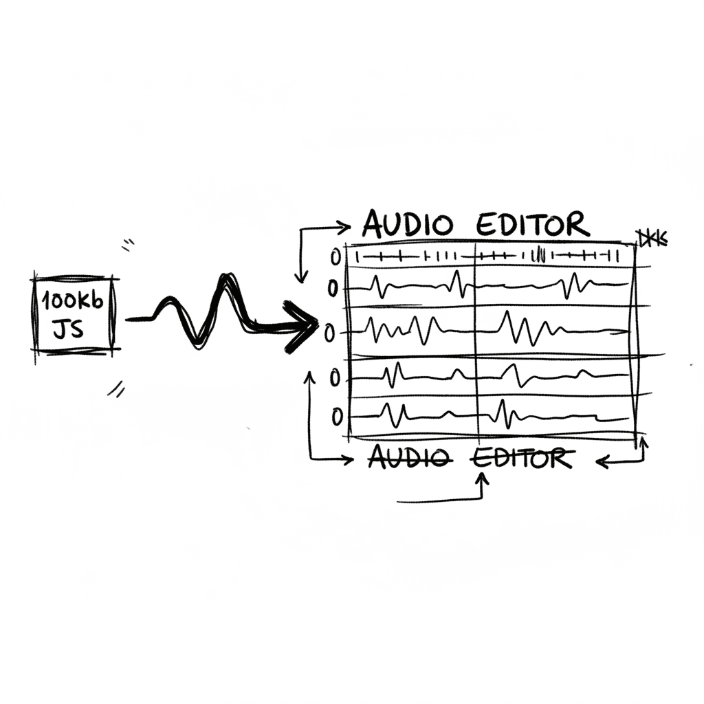
Audiomass: Multitrack Audio Editing via 100kb of Vanilla JavaScript
Audiomass is a browser-based, multitrack audio editor that operates entirely client-side with a remarkably small 100kb footprint (audiomass.co). It provides a workflow reminiscent of classic editors l
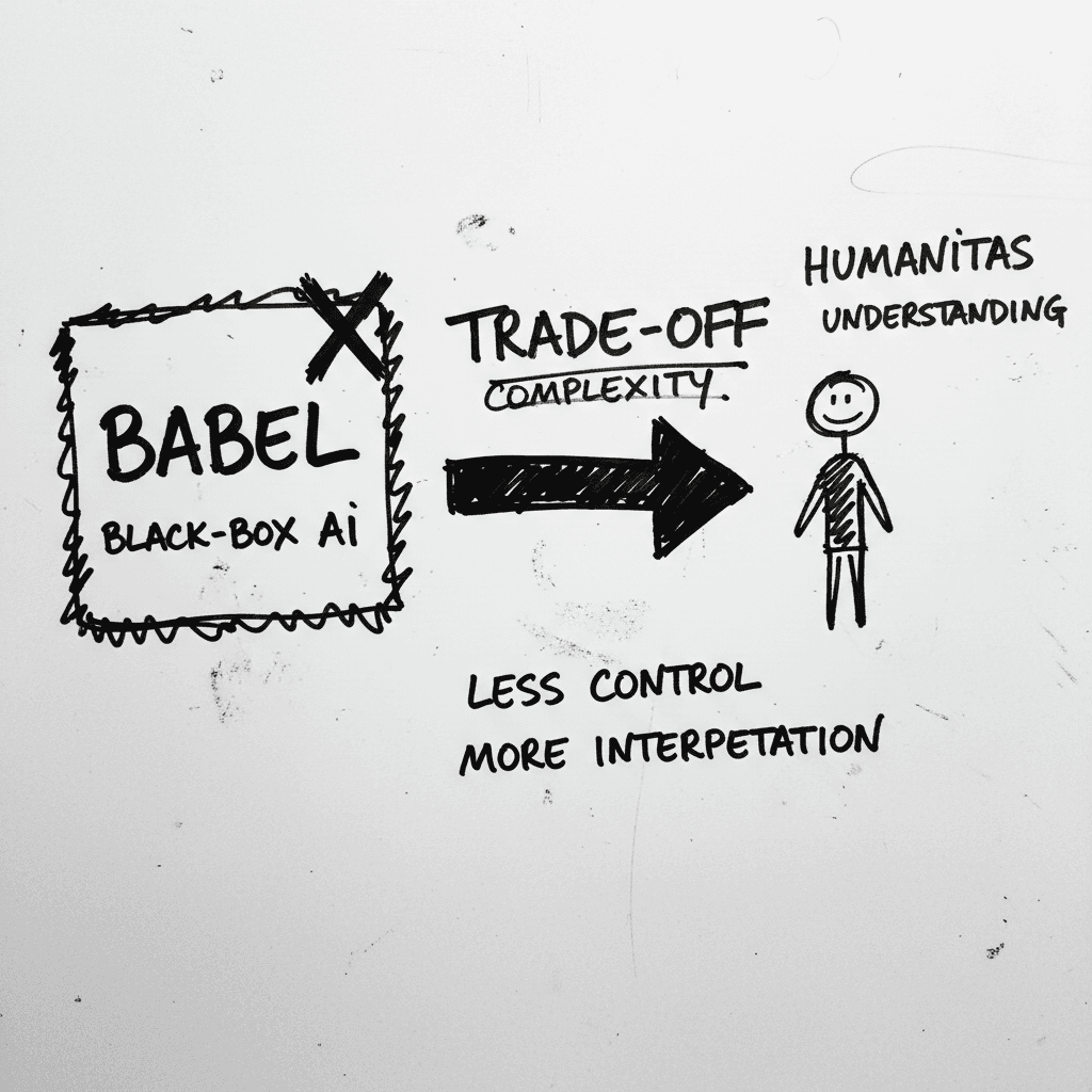
Magnifica Humanitas: The Vatican’s Framework for the GPT-5 Era
The document, signed May 15 and officially released today, was presented at the Vatican alongside Christopher Olah, co-founder of Anthropic and lead of its interpretability team (ncronline.org, Forbes
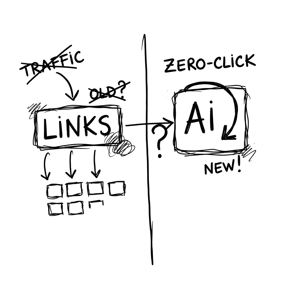
The Zero-Click Economy: Kagi Search vs. Google AI Mode
Google has effectively pivoted to an "answer engine" where Gemini 3.5 Flash provides conversational summaries, while Kagi remains the primary refuge for users seeking a human-centric, ad-free index. W
Stay Ahead of AI Adoption Trends
Get our latest reports and insights delivered to your inbox. No spam, just data.